Introduction to VLSI Design:
Definitions: VLSI = Very Large Scale Integration
VLSI > 10k tranzistors on a chip
LSI > 1K tranzistors on a chip
MSI > 100 tranzistors on a chip
SSI > 10 tranzistors on a chip
Nota bene: Different sources = different definitions!
Terminology differences:
TRANSISTOR COUNT
versus
GATE COUNT
What is the difference:
Silicon
NMOS 1+FANIN
PMOS 2*FANIN
ECL 3+FANIN
GaAs
E/D-MESFET 1+FANIN
Nota bene: The term DEVICE has two meanings
TRANSISTORS
Or
GATE
The VLSI Design Methodologies:
- Geometric symbols
FC or FULL CUSTOM (designing N mask levels)
- Logic symbols
SC or STANDARD CELL (designing N mask levels)
Semi-custom versus macro-cell
GA or GATE ARRAYS (designing only 1 or 2 wiring
related mask levels; other mask levels
prefabricated)
GTL elements versus RTL elements
PL or PROGRAMMBLE LOGIC
(all mask levels prefabricated)
GTL elements versus RTL elements
- Behavior symbols
ST or SILICOM TRANSLATION
(translation to any of the above)
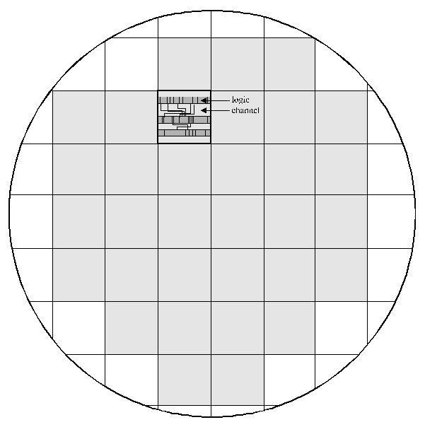
Figure 4.1.
Sketch of the semiconductor wafer containing a large number of chips designed using the SC (Standard Cells) VLSI methodology. The channels containing standard cells have the same width, and are not equidistant. The channels containing connections have varying width-their widths are governed by the number and the structure of connections that have to be made. They take up a relatively small proportion of the chip area (around 33% in this sketch). The total chip area is as big as the implemented logic requires (the chip utilization is always close to 100%)
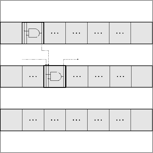
Figure 4.2. Sketch of the chip designed using GA (Gate Array) VLSI methodology. The channels that contain the gates are of the same width, and are equidistant. The channels that contain the connection are also of the same width-their widths are predetermined during the prefabrication process. They take up more chip area (around 50% of the sketch). The total chip area is always bigger then the area required by the logic, because the prefabricated chips of standard dimensions are used (the chip utilization is virtually always below 100%-the designers are usually very happy if they reach 90%)
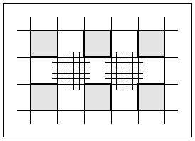
Figure 4.3. Sketch of the chip designed using the PL (Programmable Logic) VLSI methodology. The areas containing the macrocells (shaded) take up only the fraction of the chip area (around 25% in the sketch). The channels containing the connections take up the rest of the area (around 75% in the sketch), and their intersections contain the interconnection networks that are controlled using either RAM (XILINX) or ROM (ALTERA) memory elements. The sketch shows one of the many possible internal architectures that are frequently implemented. The total chip area is always bigger than area required by logic, because the prefabricated chip of standard dimensions are used (the chip utilization is virtually always below 100%-the designers are usually very happy if they reach 80%)
The Programmable Logic VLSI:
1. Altera(Untel)
2. Xilinx
3. Cypress + Actel + Lattice
4. Plessey + Ferranti
The ALTERA Approach to PL VLSI:
- Hardware
4 families
- Software
4 corresponding families, all of the same structure
- Schematic entry
- Logic and timing testing
- Placements and routing (trivial)
- Programmation (JEDEC)
- Board population and testing
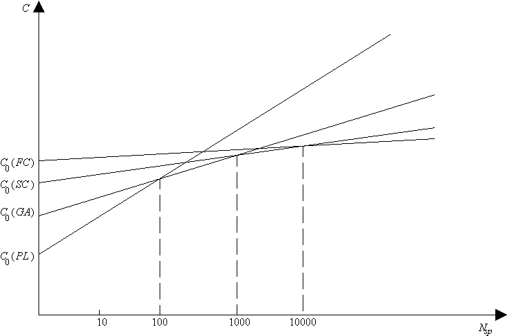
Figure 4.4.
The dependency of the cost with respect to the number of chips manufactured. The C-axis represents the total cost of the design and manufacturing processes, for the series comprising of Nsp VLSI chips. The value C0 that corresponds to Nsp = 0 represents the sum of the two components. They are: the cost of the design, and the cost of all the masks that have to be made after the design is complete.
The FULL CUSTOM Approach to VLSI
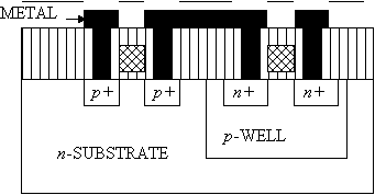
Each device technology and each design technique are characterized with a certain number of VLSI mask levels.
Different VLSI mask levels correspond to different technological actions in the fabrication processes
Each mask level is defined via a set of non-overlapping poligons. Poligons from different mask levels do overlap, according to some min/max rules
With the structured design approaches, the minimal geometry (lambda) is defined. The min/max values of overlapping are defined via the lambda rules
|
CROSS SECTION OF PHYSICAL STRUCTURE |
|
(SIDE VIEW) |
MASK (TOP VIEW) |
|
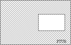
PTUB MASK |
|
|
|
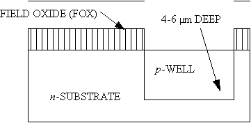
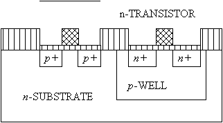
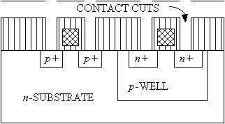
Figure 4.5a. The processes of implementation of a silicon CMOS transistor, and geometric structure of the corresponding VLSI masks: mask #1.
|
CROSS SECTION OF PHYSICAL STRUCTURE |
|
(SIDE VIEW) |
MASK (TOP VIEW) |
|
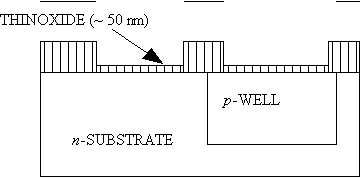
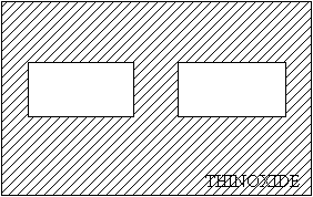
THINOXIDE MASK |
|
|
|
Figure 4.5b. The processes of implementation of a silicon CMOS transistor, and the geometric structure of the corresponding VLSI masks: mask #2.
|
CROSS SECTION OF PHYSICAL STRUCTURE |
|
(SIDE VIEW) |
MASK (TOP VIEW) |
|
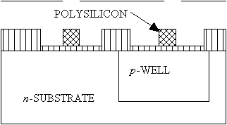
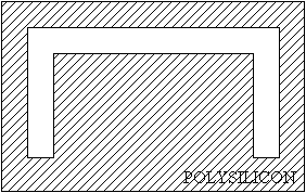
POLYSILICON MASK |
|
|
|
Figure 4.5c. The processes of implementation of a silicon CMOS transistor, and the geometric structure of corresponding VLSI masks: mask #3
|
CROSS SECTION OF PHYSICAL STRUCTURE |
|
(SIDE VIEW) |
MASK (TOP VIEW) |
|
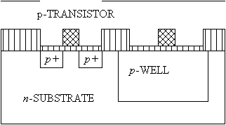
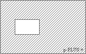
p-PLUS MASK (POSITIVE) |
|
|
|
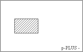
Figure 4.5d. The processes of implementation of a silicon CMOS transistor, and the geometric structure of corresponding VLSI masks: mask #4
|
CROSS SECTION OF PHYSICAL STRUCTURE |
|
(SIDE VIEW) |
MASK (TOP VIEW) |
|
p-PLUS MASK (NEGATIVE) |
|
 |
|
Figure 4.5e. The processes of implementation of a silicon CMOS transistor, and the geometric structure of corresponding VLSI masks: mask #5
|
CROSS SECTION OF PHYSICAL STRUCTURE |
|
(SIDE VIEW) |
MASK (TOP VIEW) |
|
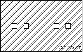
CONTACT MASK |
|
 |
|
Figure 4.5f. The processes of implementation of a silicon CMOS transistor, and the geometric structure of corresponding VLSI masks: mask #6
|
CROSS SECTION OF PHYSICAL STRUCTURE |
|
(SIDE VIEW) |
MASK (TOP VIEW) |
|
|
METAL MASK |
|
 |
|
|
Figure 4.5g. The processes of implementation of a silicon CMOS transistor, and the geometric structure of corresponding VLSI masks: mask #7
NO. MASK FEATURE DIMENSION
1 Thinox A1. Minimum thinox width 2l
A2. Minimum thinox spacing ( to ,
to ,  to
to  ) 2l
) 2l
A3. Minimum p-thinox to n-thinox spacing 8l
2 p-well B1. Minimum p-well width 4l
B2. Minimum p-well spacing (wells at same potential) 2l
B3. Minimum p-well spacing (wells at different potential) 6l
B4. Minimum distance to internal thinox 3l
B5. Minimum distance to external thinox 5l
3 Poly C1. Minimum poly width 2l
C2. Minimum poly spacing 2l
C3. Minimum poly to thinox spacing l
C4. Minimum poly gate extension 2l
C5. Minimum thinox source/drain extension 2l
4 p-plus D1. Minimum overlap of thinox 1,5–2l
D2. Minimum p-plus spacing 2l
D3. Minimum gate overlap or distance to gate edge 1,5–2l
D4. Minimum spacing to unrelated thinox 1,5–2l
5 Contact E1. Minimum contact area 2l ´ 2l
E2. Minimum contact to contact spacing 2l
E3. Minimum overlap of thinox or poly over contact l
E4. Minimum spacing to gate poly 2l
E5. source/drain contact
E6. source/drain contact
E7.  contact See reference [WesEsh85]
E8.  contact
E9. Split contact
E10. Split contact
6 Metal F1. Minimum metal width 2–3l
F2. Minimum metal spacing 3l
F3. Minimum metal overlap of contact l
Figure 4.6. The Lambda rules that have to be satisfied when forming the geometrical structures for various mask levels in the implementation of a silicon CMOS transistor.
Examples:
lambda = 3 microns for the first 32-bit Silicon RISC
lambda = 1 microns for the first 32-bit GaAs RISC
lambda < 1 microns for the modern submicron
superscalar/superpipelined RISC maschines
Advantages of the full custom approach:
Chip area
(can be minimized by carefull design)
Speed (direct and indirect impacts)
Disipation (the application dependent issue)
Price of the fabrication (2n; for n between 2 and 3)
Drawbacks
:
Engineering time (can be maximized by careful design)
Price of the design (culture dependant)
Long idea to market time (the 6/50 rule)
Unfavorable learning curve (interdisciplinary
knowledge required)
What is being designed with the FC method:
Standard cells for the FC VLSI
Semi- custom standard cells
N-input one-bit logic gates
One-bit flip-flops
Macro-cell standard cells
(De)multiplexers, (De)coders,…
Adders, multipliers,…
Standard cell extensions for the existing
standard cell families
Open CAD versus closed CAD
Highly-repetitive on-chip structures
Memory chips,…
Systolic arrays,…
Not so highly-repetitive structures,
to be fabricated in enormous quantities
Popular microprocessors
Specialized microcontrollers
None of the above, but simple
Glue logic
Small specialized logic
What is being designed with the SC method:
- Structures which are not "simple"
- Structures which are not to be
fabricated in enormous quantities
Examples:
- Prototype of the first 32=bit GaAs RISC for DARPA
- Specialized I/O RISCs
Comments:
- The 95/5 without_FC rule
- The 95/5 per_project versus per_chip rule
Examples:
The TANNER RESEARCH Tools for MOSIS
Orcad (S-Edit) + GateSim + L-Edit + the SCMOS cell family
The CADDAS Tools of RCA
Valid + Logsim + MPD2D+12 standard cells families