Veljko Milutinovic
MPS:
Understanding the Issues
vm@etf.rs
Advanced RISC Microprocessors
The DEC Alpha AXP
Digital Equipment Corporation.
The first product realizing the Alpha AXP architecture is labeled 21064.
The Alpha is a 64-bit RISC-type microprocessor.
The PowerPC Family
IBM, Motorola, and Apple.
The first PowerPC implementation is the PowerPC 601 microprocessor
(also called MPC 601 by Motorola, and PPC 601 by IBM).
The Sun SPARC Family
Sun Microsystems.
The name SPARC stands for scalable processor architecture.
The SPARC architecture follows the Berkeley RISC design philosophy.
The MIPS Rx000 Family
MIPS Computer Systems.
The MIPS acronym stands for microprocessor without interlocked pipeline stages.
The MIPS system originated at Stanford University in the early eighties.
The Intel i860/i960 Family
The i860 RISC was first announced in 1989.
It features on-chip FPU, dual cache, and graphics unit
(the first microprocessor with such a feature).
The Motorola M88000 Family
The first members of the M88000 family are the MC88100 and MC88200.
They were followed by the RISC MC88110,
which is a two-issue superscalar.
The HP Precision Architecture Family
The PA-RISC architecture was designed to be scaleable
across technologies, cost ranges, performance ranges,
and to provide price-performance advantages.
|
Company |
Internet URL of microprocessor family home page |
|
IBM |
http://www.chips.ibm.com/products/ppc/DataSheets/techlibsheets.html |
|
Motorola |
http://www.mot.com/SPS/PowerPC |
|
DEC |
http://www.europe.digital.com/semiconductor/alpha.htm |
|
Sun |
http://www.sun.com/sparc |
|
MIPS |
http://www.sgi.com/MIPS/products/index.html |
|
Hewlett-Packard |
http://hpcc920.external.hp.com/computing/framed/technology/micropro |
|
AMD |
http://www.amd.com/K6 |
|
Intel |
http://www.intel.com/english/PentiumII/zdn.htm |
[Stojanovic96] Stojanovic, M., "Advanced RISC Microprocessors," Internal Report, Department of Computer Engineering,
School of Electrical Engineering, University of Belgrade, Belgrade, Serbia, Yugoslavia, December 1995.
Microprocessors and Their Primary Manufacturers
(source: [Prvulovic97])
|
Microprocessor |
Company |
|
PowerPC 601 |
IBM, Motorola |
|
PowerPC 604e |
IBM, Motorola |
|
PowerPC 620* |
IBM, Motorola |
|
Alpha 21064* |
Digital Equipment Corporation (DEC) |
|
Alpha 21164* |
Digital Equipment Corporation (DEC) |
|
Alpha 21264* |
Digital Equipment Corporation (DEC) |
|
SuperSPARC |
Sun Microelectronics |
|
UltraSPARC-I* |
Sun Microelectronics |
|
UltraSPARC-II* |
Sun Microelectronics |
|
R4400* |
MIPS Technologies. |
|
R10000* |
MIPS Technologies. |
|
PA7100 |
Hewlett-Packard |
|
PA8000* |
Hewlett-Packard |
|
PA8500* |
Hewlett-Packard |
|
MC88110 |
Motorola |
|
AMD K6 |
Advanced Micro Devices (AMD) |
|
i860 XP |
Intel |
|
Pentium II |
Intel |
Legend: * 64-bit microprocessors, all others are 32-bit microprocessors.
Microprocessor Technology
(sources: [Prvulovic97], [Stojanovic95])
|
Microprocessor |
Technology |
Transistors |
Frequency [MHz] |
Package |
|
PowerPC 601 |
0.6 m m, 4 L, CMOS |
2,800,000 |
80 |
304 PGA |
|
PowerPC 604e |
0.35 m m, 5 L, CMOS |
5,100,000 |
225 |
255 BGA |
|
PowerPC 620 |
0.35 m m, 4 L, CMOS |
7,000,000 |
200 |
625 BGA |
|
Alpha 21064 |
0.7 m m, 3 L, CMOS |
1,680,000 |
300 |
431 PGA |
|
Alpha 21164 |
0.35 m m, 4 L, CMOS |
9,300,000 |
500 |
499 PGA |
|
Alpha 21264 |
0.35 m m, 6 L, CMOS |
15,200,000 |
500 |
588 PGA |
|
SuperSPARC |
0.8 m m, 3 L, CMOS |
3,100,000 |
60 |
293 PGA |
|
UltraSPARC-I |
0.4 m m, 4 L, CMOS |
5,200,000 |
200 |
521 BGA |
|
UltraSPARC-II |
0.35 m m, 5 L, CMOS |
5,400,000 |
250 |
521 BGA |
|
R4400 |
0.6 m m, 2 L, CMOS |
2,200,000 |
150 |
447 PGA |
|
R10000 |
0.35 m m, 4 L, CMOS |
6,700,000 |
200 |
599 LGA |
|
PA7100 |
0.8 m m, 3 L, CMOS |
850,000 |
100 |
504 PGA |
|
PA8000 |
0.35 m m, 5 L, CMOS |
3,800,000 |
180 |
1085 LGA |
|
PA8500 |
0.25 m m, ? L, CMOS |
>120,000,000 |
250 |
? |
|
MC88110 |
0.8 m m, 3 L, CMOS |
1,300,000 |
50 |
299 |
|
AMD K6 |
0.35 m m, 5 L, CMOS |
8,800,000 |
233 |
321 PGA |
|
i860 XP |
0.8 m m, 3 L, CHMOS |
2,550,000 |
50 |
262 PGA |
|
Pentium II |
0.35 m m, ? L, CMOS |
7,500,000 |
300 |
242 SEC |
Legend:
x L—x-layer metal (x = 2, 3, 4);
PGA—pin grid array;
BGA—ball grid array;
LGA—land grid array;
SEC—single edge contact;
Microprocessor Architecture
(sources: [Prvulovic97], [Stojanovic95])
|
Microprocessor |
IU registers |
FPU registers |
VA |
PA |
EC Dbus |
SYS Dbus |
|
PowerPC 601 |
32´ 32 |
32´ 64 |
52 |
32 |
none |
64 |
|
PowerPC 604e |
32´ 32 +RB(12) |
32´ 64 +RB(8) |
52 |
32 |
none |
64 |
|
PowerPC 620 |
32´ 64 +RB(8) |
32´ 64 +RB(8) |
80 |
40 |
128 |
128 |
|
Alpha 21064 |
32´ 64 |
32´ 64 |
43 |
34 |
128 |
128 |
|
Alpha 21164 |
32´ 64 +RB(8) |
32´ 64 |
43 |
40 |
128 |
128 |
|
Alpha 21264 |
32´ 64 +RB(48) |
32´ 64 +RB(40) |
? |
44 |
128 |
128 |
|
SuperSPARC |
136´ 32 |
32´ 32* |
32 |
36 |
none |
64 |
|
UltraSPARC-I |
136´ 64 |
32´ 64 |
44 |
36 |
128 |
128 |
|
UltraSPARC-II |
136´ 64 |
32´ 64 |
44 |
36 |
128 |
128 |
|
R4400 |
32´ 64 |
32´ 64 |
40 |
36 |
128 |
64 |
|
R10000 |
32´ 64 +RB(32) |
32´ 64 +RB(32) |
44 |
40 |
128 |
64 |
|
PA7100 |
32´ 32 |
32´ 64 |
64 |
32 |
? |
? |
|
PA8000 |
32´ 64 +RB(56) |
32´ 64 |
48 |
40 |
64 |
64 |
|
PA8500 |
32´ 64 +RB(56) |
32´ 64 |
48 |
40 |
64 |
64 |
|
MC88110 |
32´ 32 |
32´ 80 |
32 |
32 |
none |
? |
|
AMD K6 |
8´ 32 +RB(40) |
8´ 80 |
48 |
32 |
64 |
64 |
|
i860 XP |
32´ 32 |
32´ 32* |
32 |
32 |
none |
? |
|
Pentium II |
? |
8´ 80 |
48 |
36 |
64 |
64 |
Legend:
IU—integer unit;
FPU—floating point unit;
VA—virtual address [bits];
PA—physical address [bits];
EC Dbus—external cache data bus width [bits];
SYS Dbus—system bus width [bits];
RB—rename buffer [size expressed in the number of registers];
* Can also be used as a 16´ 64 register file.
Microprocessor ILP Features
(sources: [Prvulovic97], [Stojanovic95])
|
Microprocessor |
ILP issue |
LSU units |
IU units |
FPU units |
GU units |
|
PowerPC 601 |
3 |
1 |
1 |
1 |
0 |
|
PowerPC 604e |
4 |
1 |
3 |
1 |
0 |
|
PowerPC 620 |
4 |
1 |
3 |
1 |
0 |
|
Alpha 21064 |
2 |
1 |
1 |
1 |
0 |
|
Alpha 21164 |
4 |
1 |
2 |
2 |
0 |
|
Alpha 21264 |
4 |
1 |
4 |
2 |
0 |
|
SuperSPARC |
3 |
0 |
2 |
2 |
0 |
|
UltraSPARC-I |
4 |
1 |
4 |
3 |
2 |
|
UltraSPARC-II |
4 |
1 |
4 |
3 |
2 |
|
R4400 |
1* |
0 |
1 |
1 |
0 |
|
R10000 |
4 |
1 |
2 |
2 |
0 |
|
PA7100 |
2 |
1 |
1 |
3 |
0 |
|
PA8000 |
4 |
2 |
2 |
4 |
0 |
|
PA8500 |
4 |
2 |
2 |
4 |
0 |
|
MC88110 |
2 |
1 |
3 |
3 |
2 |
|
AMD K6 |
6** |
2 |
2 |
1 |
1*** |
|
i860 XP |
2 |
1 |
1 |
2 |
1 |
|
Pentium II |
5** |
? |
? |
? |
? |
Legend:
ILP = instruction level parallelism;
LSU = load/store or address calculation unit;
IU = integer unit;
FPU = floating point unit;
GU = graphics unit;
* Superpipelined;
** RISC instructions, one or more of them are needed to emulate an 80x86 instruction;
*** MMX (multimedia extensions) unit.
Microprocessor Cache Memory
(sources: [Prvulovic97], [Stojanovic95])
|
Microprocessor |
L1 Icache, Kbytes |
L1 Dcache, Kbytes |
L2 cache, Kbytes |
|
PowerPC 601 |
32, 8WSA, UNI |
— |
|
PowerPC 604e |
32, 4WSA |
32, 4WSA |
— |
|
PowerPC 620 |
32, 8WSA |
32, 8WSA |
—* |
|
Alpha 21064 |
8, DIR |
8, DIR |
—* |
|
Alpha 21164 |
8, DIR |
8, DIR |
96, 3WSA* |
|
Alpha 21264 |
64, 2WSA |
64, DIR |
—* |
|
SuperSPARC |
20, 5WSA |
16, 4WSA |
— |
|
UltraSPARC—I |
16, 2WSA |
16, DIR |
—* |
|
UltraSPARC—II |
16, 2WSA |
16, DIR |
—* |
|
R4400 |
16, DIR |
16, DIR |
—* |
|
R10000 |
32, 2WSA |
32, 2WSA |
—* |
|
PA7100 |
0 |
—** |
|
PA8000 |
0 |
—** |
|
PA8500 |
512, 4WSA |
1024, 4WSA |
— |
|
MC88110 |
8, 2WSA |
8, 2WSA |
— |
|
AMD K6 |
32, 2WSA |
32, 2WSA |
—* |
|
i860 XP |
16, 4WSA |
16, 4WSA |
— |
|
Pentium II |
16, ? |
16. ? |
512, ?*** |
Legend:
Icache—on-chip instruction cache;
Dcache—on-chip data cache;
L2 cache—on chip L2 cache;
DIR—direct mapped;
xWSA—x-way set associative;
UNI—unified L1 instruction and data cache;
* on-chip cache controller for external L2 cache;
** on-chip cache controller for external L1 cache;
*** L2 cache is in the same package, but on a different silicon die.
Miscellaneous Microprocessor Features
(source: [Prvulovic97])
|
Microprocessor |
ITLB |
DTLB |
BPS |
|
PowerPC 601 |
256, 2WSA, UNI |
—* |
|
PowerPC 604e |
128, 2WSA |
128, 2WSA |
512 ´ 2BC |
|
PowerPC 620 |
128, 2WSA |
128, 2WSA |
2048 ´ 2BC |
|
Alpha 21064 |
12 |
32 |
4096 ´ 2BC |
|
Alpha 21164 |
48 ASSOC |
64 ASSOC |
ICS ´ 2BC |
|
Alpha 21264 |
? |
? |
? |
|
SuperSPARC |
64 ASOC, UNI |
? |
|
UltraSPARC-I |
64 ASOC |
64 ASOC |
ICS ´ 2BC |
|
UltraSPARC-II |
64 ASOC |
64 ASOC |
ICS ´ 2BC |
|
R4400 |
48 ASOC |
48 ASOC |
— |
|
R10000 |
64 ASOC |
64 ASOC |
? ´ 2BC |
|
PA7100 |
16 |
120 |
? |
|
PA8000 |
4 |
96 |
256 ´ 3BSR |
|
PA8500 |
160, UNI |
>256 ´ 2BC |
|
MC88110 |
40 |
40 |
? |
|
AMD K6 |
64 |
64 |
8192 ´ 2BC, 16´ RAS |
|
i860 XP |
64, UNI |
? |
|
Pentium II |
? |
? |
? |
Legend:
ITLB—translation lookaside buffer for code [entries];
DTLB—translation lookaside buffer for data [entries];
2WSA—two-way set associative; ASOC = fully associative;
UNI—unified TLB for code and data;
BPS—branch prediction strategy;
2BC—two-bit counter;
3BSR—three bit shift register;
RAS—return address stack;
ICS—instruction cache size (2BC for every instruction in the instruction cache);
* hinted instructions available for static branch prediction.
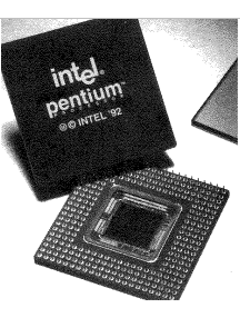
intel®
PENTIUM™ PROCESSOR
Binary Compatible with Large Software Base
- MS-DOS, Windows, OS/2, UNIX SVR4, NeXTstep 486, Solaris 2.0
32-bit Microprocessor
- 32-bit Addressing
- 64-bit Data Bus
Superscalar architecture
- Two pipelined integer units
- Under one Clock per Instruction
- Pipelined Floating Point Unit
Separate Code and Data Caches
- 8K Code, 8K Write Back Data
- 2-way 32-byte Line Size
- Software Transparent
- MESI Cache Consistency Protocol
Advanced Design Features
273-Pin Grid Array Package
BiCMOS Silicon Technology
Increased Page Size
- 4M for Increased TLB Hit Rate
Multi-Processor Support
- Multiprocessor Instructions
- Support for Second Level Cache
Internal Error Detection
- Functional Redundancy Checking
- Built in Self Test
- Parity testing and checking
IEEE 1149.1 Boundary Scan Compatibility
Performance Monitoring
- Counts Occurrence of Internal Events
- Traces Execution through Pipelines
|
The Pentium processor provides the new generation of power for high-end workstations and servers. The Pentium processor is compatible with the entire installed base of applications for DOS, Windows, OS/2, and UNIX. The Pentium processor’s superscalar architecture can execute two instructions per clock cycle. Branch prediction and separate caches also increase performance. The pipelined floating point unit of the Pentium processor delivers workstation level performance. Separate code and data caches reduce cache conflicts while remaining software transparent. The Pentium processor has
3.1 million transistors and is built on Intel’s .8 micron BiCMOS silicon technology. |
|
Pentium™ Processor Pinout (Top View)
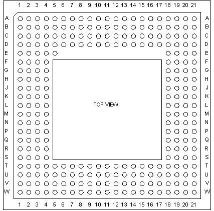
Figure MPSS1: Pentium pin layout (source: [Intel93])
Legend: Self-explanatory.
Architecture Overview:
100% binary compatible with ancestors.
Enhancements and additions to i486:
- Superscalar Architecture
- Dynamic Branch Prediction
- Pipelined Floating-Point Unit
- Improved Instruction Execution Time
- Separate 8K Code and Data Caches
- Writeback MESI Protocol (Data Caches)
- 64-Bit Data Bus
- Bus Cycle Pipelining
- Address Parity
- Internal Parity Checking
- Functional Redundancy Checking
- Execution Tracking
- Performance Monitoring
- IEEE 1149.1 Boundary Scan
- System Management Mode
- Virtual Mode Extensions
New instructions
to accommodate the additional functionality.
The MMU fully compatible with i386 and i486.
The floating-point unit completely redesigned,
compared with i486.
Pin Functional Grouping
|
Function |
Pins |
|
Clock |
CLK |
|
Initialization |
RESET, INIT |
|
Address Bus |
A31–A3, BE7#–BE0# |
|
Address Mask |
A20M# |
|
Data Bus |
D63–D0 |
|
Address Parity |
AP, APCHK# |
|
Data Parity |
DP7–DP0, PCHK#, PEN# |
|
Internal Parity Error |
IERR# |
|
System Error |
BUSCHK# |
|
Bus Cycle Definition |
M/IO#, D/C#, W/R#, CACHE#, SCYC, LOCK# |
|
Bus Control |
ADS#, BRDY, NA# |
|
Page Cacheability |
PCD, PWT |
|
Cache Control |
KEN#, WB/WT# |
|
Cache Snooping/Consistency |
AHOLD, EADS#, HIT#, HITM#, INV |
|
Cache Flush |
FLUSH# |
|
Write Ordering |
EWBE# |
|
Bus Arbitration |
BOFF#, BREQ, HOLD, HLDA |
|
Interrupts |
INTR, NMI |
|
Floating Point Error Reporting |
FERR#, IGNNE# |
|
System Management Mode |
SMI#, SMIACT# |
|
Functional Redundancy Checking |
FRCMC# (IERR#) |
|
TAP Port |
TCK, TMS, TDI, TDO, TRST# |
|
Breakpoint/Performance Monitoring |
PM0/BP0, PM1/BP1, BP3–2 |
|
Execution Tracing |
BT3–BT0, IU, IV, IBT |
|
Probe Mode |
R/S#, PRDY |
Figure MPSS2: Pentium pin functions (source: [Intel93])
Legend:
TAP—Processor boundary scan.
Pentium™ Processor Block Diagram

Figure MPSS3: Pentium block digaram (source: [Intel93])
Legend:
TLB—Translation Lookaside Buffer.
Intel486™ Pipeline Execution
|
PF |
I1 |
I2 |
I3 |
I4 |
|
|
|
|
|
D1 |
|
I1 |
I2 |
I3 |
I4 |
|
|
|
|
D2 |
|
|
I1 |
I2 |
I3 |
I4 |
|
|
|
EX |
|
|
|
I1 |
I2 |
I3 |
I4 |
|
|
WB |
|
|
|
|
I1 |
I2 |
I3 |
I4 |
Pentium™ Pipeline Execution
|
PF |
I1 |
I3 |
I5 |
I7 |
|
|
|
|
|
|
I2 |
I4 |
I6 |
I8 |
|
|
|
|
|
D1 |
|
I1 |
I3 |
I5 |
I7 |
|
|
|
|
|
|
I2 |
I4 |
I6 |
I8 |
|
|
|
|
D2 |
|
|
I1 |
I3 |
I5 |
I7 |
|
|
|
|
|
|
I2 |
I4 |
I6 |
I8 |
|
|
|
EX |
|
|
|
I1 |
I3 |
I5 |
I7 |
|
|
|
|
|
|
I2 |
I4 |
I6 |
I8 |
|
|
WB |
|
|
|
|
I1 |
I3 |
I5 |
I7 |
|
|
|
|
|
|
I2 |
I4 |
I6 |
I8 |
Figure MPSS4: Intel 486 pipeline versus Pentium pipeline (source: [Intel93])
Legend:
PF—Prefetch;
D1/2—Decoding 1/2;
EX—Execution;
WB—Writeback.
Instructions Prefetch:
In the PF stage,
two independent prefetch buffers
and the branch target buffer
operate in conjunction.
One prefetch buffer requests prefetches
at any given time.
Prefetches are requested sequentially,
until a branch is fetched.
- If a branch is fetched,
BTB predicts whether it will be taken or not.
- If predicted "not taken,"
prefetch requests continue sequentially.
If predicted "taken,"
the other prefetch buffer is enabled
and begins to prefetch as if the branch was taken
(if mispredicted, instruction pipes are flushed).
Pipeline Stage D1 (Decode 1):
Two parallel decoders attempt to decode and issue
the next two sequential instructions.
The decoders determine whether one or two instructions can be issued, based on the instructions pairing rules.
If prefixes, an extra D1 clock is needed.
Prefixes go only to the u-pipeline,
one per clock cycle;
base instruction is issued and paired with others,
after all prefixes have been issued.
Pipeline Stage D2 (Decode 2):
The addresses of memory resident operands
are calculated.
One clock cycle for both address calculations,
in displacement + immediate data instructions,
and base + index addressing instructions
(i486 requires two cycles).
Pipeline Stage EX (Execute):
Used for both, ALU operations and data cache access.
Two clocks if both present,
ALU operation + data cache access.
All u-pipe instructions,
and all v-pipe instructions except conditional branches,
verified for correct branch prediction.
Pipeline Stage WB (Writeback):
Instructions enabled to modify processor state,
and to complete the execution.
The v-pipe conditional branches
verified for correct branch prediction.
Stall:
- Instructions in both pipes may stall
due to certain conditions.
- Stages D1 and D2 always entered and left at unison.
This means,
if one stalls, the other one will stall, too.
- Stage EX always entered in unison.
If u-pipe is stalled, the v-pipe is stalled, too.
If v-pipe is stalled, the u-pipe proceeds.
No successive instructions into EX
before both pipes advanced to WB.
Instruction Pairing Rules:
Conditions for pairing:
(a) Both must be "simple"
(b) No RAW or WAW dependencies
(c) Neither can contain both,
a displacement and an immediate
(d) Instructions with prefixes
(other than 0f of JCC)
can occur only in the u-pipe.
- Exceptions: business as usual!
- Simple instructions are entirely hardwired,
and execute in one clock,
except ALU mem, reg (2 cycles)
and ALU reg, mem (3 cycles).
- Simple:
mov, alu, inc, dec, push, pop, lea, jmp, call, jccnear, nop.
Branch Prediction:
BTB used to predict
the outcome of branch instructions.
Current address in D1 is applied to BTB.
If hit,
the assumption is that the branch will be taken
(if the assumption is correct,
execution goes without stalls and flushes).
If miss,
the assumption is the branch will not be taken.
A mispredicted branch
(weather BTB hit or miss)
causes the pipeline to be flushed.
The number of delay clocks
depends on the branch type.
Write Buffers + Memory Ordering:
Two write buffers (one per pipe)
to enhance the performance of
consecutive writes to memory.
Can be filled in one clock,
by two simultaneous write misses
in the two instruction pipes.
- Writes into these buffers are driven out
on the external bus,
using the strong write ordering.
Example:
Loop for computing prime numbers:
for(k=i+prime; k<=SIZE; k+=prime)
flags[k]=FALSE;
- Allocation:
prime - ecx
k - edx
FALSE - al
- Assembly code:
inner_loop:
mov byte ptr flags[edx], al
add edx, ecx
cmp edx, FALSE
jle inner_loop
- Pairing: mov+add and cmp+jle
Execution time:
Texe[Pentium (with branch prediction)]=2
Texe[i486]=6
External Event Synchronization:
When the system changes the value of
NMI, INTR, FLUSH#, SMI#, or INIT,
as the result of executing an OUT instruction,
these inputs must be at a valid state
three clocks before BRDY# is returned,
to ensure that the new value is recognized,
before the next instruction is executed.
An OUT instruction can be used
to modify AZOM#.
Serializing Operations:
After executing certain instructions,
the Pentium processor serializes instruction execution.
This means that any modifications
to flags, registers, and memory,
for previous instructions are completed,
before the next instruction is fetched and executed.
The prefetch queue is flushed
as a result of the serializing operations.
The Pentium processor serializes
the instruction execution
after executing one of the instructions:
MSR (Move to Special Register),
INVD, INVLPG, IRET, IRETD, CPUID, ...
External Interrupt:
Pentium recognizes 7 external interrupts
with the following priority:
BOSCHK#
R/S#
FLUSH#
SMI#
INIT
NMI
INTR
- Interrupts are recognized
at instruction boundaries.
- In Pentium, the instruction boundary is
at the first clock in the execution stage
of the instruction pipeline.
- Before an instruction is executed,
Pentium checks if any interrupts are pending.
If yes, it flushes the instruction pipeline,
and services the interrupt.
Writeback Buffers:
In addition to two write buffers,
Pentium processor has three writeback buffers
(1-line-deep and 32-bytes-wide).
First:
A dedicated replacement writeback buffer,
which causes writebacks due to linefill
that replaces a modified line in the data cache.
Second:
One external snoop writeback buffer,
to store writeback caused by an inquire cycle
that hits a modified line in the data cache.
Third:
One internal snoop writeback buffer,
to store writebacks
caused by a modified line in the data cache.
Model Specific Registers:
Model specific registers (MSRs) are used in
execution tracing, performance monitoring, testing,
and machine check errors.
Two new instructions are used
to access these registers:
RDMSR
WRMSR
- When these instructions are executed,
the value in ECX specifies
which MSR is being accessed.
|
Value |
Register Name |
Description |
|
00H |
Machine Check Address (MCA) |
Stores address of cycle causing the execution |
|
01H |
Machine Check Type (MCT) |
Stores cycle type of cycle causing the execution |
|
0EH |
Test Register 12 (TR12) |
New feature control |
Figure MPSS5: Model specific register manipulation (source: [Intel93])
Legend:
H—Hexadecimal.
Floating-Point Unit:
On the same chip with the CPU.
Heavily pipelined.
One floating-point instruction (FPI)
in every clock cycle.
It can receive up to two FPIs,
one of which must be an exchange instruction.
Floating-Point Pipeline Stages:
The Pentium FPU has 8 pipeline stages;
the first 5 are shared with the integer unit.
The floating-point pipeline stages are:
PF Prefetch;
D1 Instruction decode;
D2 Address generation;
EX Memory and register read;
X1 Floating-point execute stage # one;
X2 Floating-point execute stage # two;
WF Rounding and writing the floating-point result
to register file;
ER Error report + update status word.
On-Chip Caches:
One 8-KB data cache and
one 8-KB code cache.
The data cache fully supports the MESI
writeback cache consistency protocol:
MESI = modified/exclusive/shared/invalid.
The data cache is configurable as write-back
or write-through,
on a line by line basis.
Parts of data memory
can be defined as non cacheable,
by software or external hardware.
The code cache is inherently write protected,
and supports a subset of MESI called SI.
Cache Organization:
Each cache is 2-way set associative,
with 128 sets in each cache,
each set containing two 32-bytes wide lines.
Both caches use the LRU replacement,
which requires one bit per set,
in each one of the caches.
Data cache includes two state bits to support MESI.
Code cache includes one state bit to support SI.
The operating modes of the caches are controlled
by the CD (code disable)
and NW (not write through) bits in CR0.
For best performance:
CD=NW=0
CD=NW=1
- To disable a cache,
one must perform two steps:
CD=NW=1
Cache must be FLUSHed.
Organization of Instruction
and Data Caches
|
|
|
MESI State |
|
|
|
|
MESI State |
|
|
|
¯ |
¯ |
|
LRU |
|
|
¯ |
¯ |
|
Set |
TAG Address |
|
|
|
¬ ® |
|
TAG Address |
|
|
|
|
WAY 0 |
|
|
|
|
|
WAY 1 |
|
|
|
Data Cache
|
|
|
State Bit (S or I) |
|
|
|
State Bit (S or I) |
|
|
|
¯ |
|
|
LRU |
|
|
¯ |
|
|
Set |
TAG Address |
|
|
|
¬ ® |
|
TAG Address |
|
|
|
|
WAY 0 |
|
|
|
|
|
WAY 1 |
|
|
|
Instruction Cache |
Figure MPSS6: Organization of instruction and data caches (source: [Intel93])
Legend:
MESI—Modified/Exclusive/Shared/Invalid;
LRU—Least Recently Used.
PCD and PWT Generation
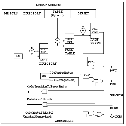
Figure MPSS7: Generation of PCD and PWT (source: [Intel93])
Legend:
PCD—a bit which controls cacheability on a page by page basis;
PWT—a bit which controls write policy for the second level caches;
PTRS—Pointers.
Page Cacheability:
Two bits for cache control (PWT and PCD)
are defined in the page table
and page directory entries.
The states of these bits are driven out
on the PWT and PCD pins
during memory access cycles.
The PWT bit controls write policy
for the second level caches:
PWT=1 (write through)
PWT=0 (write back)
- The PCD bit controls cacheability
on a page by page basis:
PCD=0 (caching enabled)
PCD=1 (caching disabled)
- The PCD bit is internally ANDed
with the KEN# signal,
to control cacheability
on the cycle by cycle basis.
Inquire Cycles:
Inquire cycles are initiated by the system
to determine if a line is present
in the code or data cache,
and what its state is
(term "snoop cycle" has the same meaning).
If the inquired (snooped) line is in data cache,
and in the "modified" state,
processor has the most recent information,
and must schedule a writeback.
Cache Flushing:
The on-chip caches can be flushed
by external hardware or internal software.
Flushing by hardware:
driving the FLUSH# pin low.
Flushing by software:
The INVD and WBINVD instructions
cause on-chip caches to be invalidated.
The MESI Protocol:
Every line in the Pentium processor data cache
is assigned a state.
This is a set of rules
by which states are assigned to cache entries (lines),
based on Pentium activities,
and the activities of other bus masters.
The states define whether a line is valid
(hit or miss),
whether it is available to other caches
(exclusive or shared),
and whether it has been modified
(modified or not).
M - Modified: An M-state line is available in ONLY one cache,
and it is also MODIFIED (different from main memory).
An M-state line can be accessed (read/written to)
without sending a cycle out on the bus.
E - Exclusive: An E-state line is also available in only one cache in the system, but the line is not MODIFIED
(i.e., it is the same as main memory).
An E-state line can be accessed (read/written to)
without generating a bus cycle.
A write to an E-state line will cause the line to become MODIFIED.
S - Shared: This state indicates that the line is potentially shared
with other caches
(i.e., the same line may exist in more that one cache).
A read to an S-state line will not generate bus activity,
but a write to a SHARED line
will generate a write-through cycle on the bus.
The write-through cycle may invalidate this line in other caches. A write to an S-state line will update the cache.
I - Invalid: This state indicates that the line is not available in the cache.
A read to this line will be a MISS,
and may cause the Pentium processor to execute LINE FILL.
A write to an INVALID line causes the Pentium processor
to execute a write-through cycle on the bus.
Figure MPSS8: Definition of states for the MESI and the SI protocols (source: [Intel93])
Legend:
LINE FILL—Fetching the whole line into the cache from main memory.
|
Present State |
Pin
Activity |
Next
State |
Description |
|
M |
n/a |
M |
Read hit;
data is provided to processor core by cache.
No bus cycle is generated. |
|
E |
n/a |
E |
Read hit;
data is provided to processor core by cache.
No bus cycle is generated. |
|
S |
n/a |
S |
Read hit;
data is provided to processor core by cache.
No bus cycle is generated. |
|
I |
CACHE# low
AND
KEN# low
AND
WB/WT# high
AND
PWT low |
E |
Data item does not exist in cache (MISS).
A bus cycle (read) will be generated
by the Pentium™ processor.
This state transition will happen
if WB/WT# is sampled high
with first BRDY# or NA#. |
|
I |
CACHE# low
AND
KEN# low
AND
(WB/WT# low
OR
PWT high) |
S |
Same as previous read miss case
except that WB/WT# is sampled low
with first BRDY# or NA#. |
|
I |
CACHE# high
AND
KEN# high |
I |
KEN# pin inactive;
the line is not intended to be cached
in the Pentium processor. |
Figure MPSS9: Data cache state transitions for UNLOCKED Pentium™ processor initiated read cycles*
(source: [Intel93])
Legend:
*—Locked accesses to the data cache will cause the accessed line to transition to the Invalid state.
|
Present State |
Pin
Activity |
Next
State |
Description |
|
M |
n/a |
M |
write hit; update data cache. No bus cycle generated to update memory. |
|
E |
n/a |
M |
Write hit; update cache only. No bus cycle generated; line is now MODIFIED. |
|
S |
PWT low
AND
WB/WT# high |
E |
Write hit; data cache updated with write data item. A write-through cycle is generated on bus to update memory and/or invalidate contents of other caches. The state transition occurs after the writethrough cycle completes on the bus (with the last BRDY#). |
|
S |
PWT low
AND
WB/WT# low |
S |
Same as above case of write to S-state line except that WB/WT# is sampled low. |
|
S |
PWT high |
S |
Same as above cases of writes to S state lines except that this is a write hit to a line in a write through page; status of WB/WT# pin is ignored. |
|
I |
n/a |
I |
Write MISS; a write through cycle is generated on the bus to update external memory. No allocation done. |
Figure MPSS10: Data cache state transitions for UNLOCKED Pentium™ processor initiated write cycles* (source: [Intel93])
Legend:
WB/WT—Writeback/Writethrough.
|
Present State |
Next
State
INV=1 |
Next
State
INV=0 |
Description |
|
M |
I |
S |
Snoop hit to a MODIFIED line indicated by HIT# and HITM# pins low. Pentium™ processor schedules the writing back of the modified line to memory. |
|
E |
I |
S |
Snoop hit indicated by HIT# pin low;
no bus cycle generated. |
|
S |
I |
S |
Snoop hit indicated by HIT# pin low;
no bus cycle generated. |
|
I |
I |
I |
Address not in cache; HIT# pin high. |
Figure MPSS11: Data cache state transitions during inquire cycles (source: [Intel93])
Legend:
INV—Invalid bit.
Reference:
[Intel93] "Pentium Processor User’s Manual," Intel, Santa Clara California, USA, 1993.
Veljko Milutinovic
MPS:
State of the Art
vm@etf.rs

Pentium MMX
New instructions of the Pentium MMX processor (source: [Intel97])
EMMS—Empty MMX state
MOVD—Move doubleword
MOVQ—Move quadword
PACKSSDW—Pack doubleword to word data (signed with saturation)
PACKSSWB—Pack word to byte data (signed with saturation)
PACKUSWB—Pack word to byte data (unsigned with saturation)
PADD—Add with wrap-around
PADDS—Add signed with saturation
PADDUS—Add unsigned with saturation
PAND—Bitwise And
PANDN—Bitwise AndNot
PCMPEQ—Packed compare for equality
PCMPGT—Packed compare greater (signed)
PMADD—Packed multiply add
PMULH—Packed multiplication
PMULL—Packed multiplication
POR—Bitwise Or
PSLL—Packed shift left logical
PSRA—Packed shift right arithmetic
PSRL—Packed shift right logical
PSUB—Subtract with wrap-around
PSUBS—Subtract signed with saturation
PSUBUS—Subtract unsigned with saturation
PUNPCKH—Unpack high data to next larger type
PUNPCKL—Unpack low data to next larger type
PXOR—Bitwise Xor
Legend:
MMX—MultiMedia eXtension.
Pentium Pro:
Basic features:
- Birthday: Nov 1, 1995 (10 months after 1st silicon)
- Technology:
BiCMOS 0.6
m m (0.3m m) 150MHz (200MHz) 5.5MTr
Performance:
6.1 (8.1) SPECint95 + 5.5 (6.8) SPECfp95
Processor: 32 bits (40 registers) BTB
Bus: 64 bits (internal and external) 50 MHz (66 MHz)
Split transactions: Decoupled address/data cycles
Superpipelined: 14 stages
Superscalar (SHT)
IFU fetches 16 bytes per clock cycle;
IDU decodes 3 instructions per clock cycle
Speculative and out-of-order execution
On-chip L1 cache: 8KB (inst) + 8KB (data) 2wSA
+ buffers for 4 outstanding misses
On-package L2 cache: 256 KB (dual-cavity PGA) 4wSA + 8ECC bits per 64 data bits
Support for SMP/DSM:
MESI + dedicated ports (1 In + 1 Out)
Dedicated I/O ports: 1 In + 1 Out (MCS + DCS)
Pentium Pro Block Diagram
(source: [Papworth96])
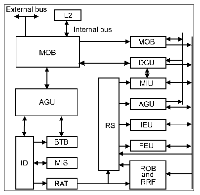
Legend:
|
AGU |
Address generation unit |
L2 |
Level-2 cache |
|
BIU |
Bus interface unit |
MIS |
Microinstruction sequencer |
|
BTB |
Branch target buffer |
MIU |
Memory interface unit |
|
DCU |
Data cache unit |
MOB |
Memory reorder buffer |
|
FEU |
Floating-point execution unit |
RAT |
Register alias table |
|
ID |
Instruction decoder |
ROB |
Reorder buffer |
|
IEU |
Integer execution unit |
RRF |
Retirement register file |
|
IFU |
Instruction fetch unit
(with I-cache) |
RS |
Reservation station |
Pentium Pro and Pentium II Bus Structures
(source: [Intel97])
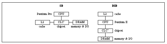
Legend:
SB—single independent bus;
DIB—dual independent bus;
CLC—control logic chipset;
L2—second level cache.
References:
[Papworth96] Papworth, D. B.,
"Tuning the Pentium Pro Microarchitecture,"
IEEE Micro, April 1996, pp. 8–16.
[Intel96] http://www.intel.com/procs/p6/p6white/index.html,
Intel, Santa Clara, California, USA, 1996.
Intel COO Craig Barrett’s Vision: 2000
1000M transistors per chip
<40 Å gate oxide thickness
<0.10 m m minimum lithographic dimension
4000 MHz
100 BIPS
Microprocessor Performance Trends
Microprocessor’s performance trend:
2´ every 18 months Þ performance at year 2001
should reach 100 SPECint95 (3500 SPECint92)
How to design future microprocessors
so as to maintain the performance trend?
Process Technology: Delay Trends
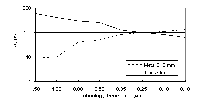
Figure MPSS1: Microprocessor chip delay trends (source: [Sheaffer96])
Legend:
Metal 2 (2 mm)—Two level metal.
Process Technology: Area Trends
|
Silicon process technology |
1.5 m m |
1.0 m m |
0.8 m m |
0.6 m m |
0.35 m m |
0.25 m m |
|
Intel386TM DX
Processor |

|
|
|
|
|
|
|
Intel486TM DX
Processor |
|
|
|
|
|
|
|
Pentium®
Processor |
|
|
|
|
|
|
|
Pentium® Pro
Processor |
|
|
|
|
est |
est |
Figure MPSU2: Microprocessor chip area trends (source: [Sheaffer96])
Legend:
est—estimated.
Frequency of Operation
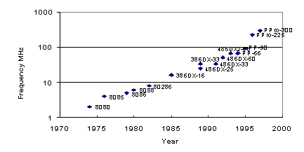
Figure MPSS3: Microprocessor chip operation frequency (source: [Sheaffer96])
Legend:
PP—Pentium Processor;
PPro—Pentium Pro Processor.
Microprocessor Complexity
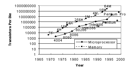
Figure MPSS4: Microprocessor and memory complexity (source: [Sheaffer96])
Brainiacs and Speedemons
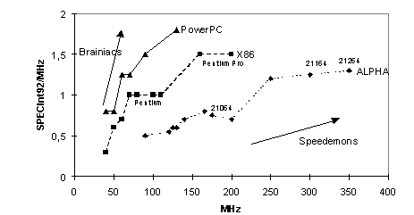
Figure MPSS5: Microprocessor sophistication (source: [Sheaffer96])
Current Trends in Design
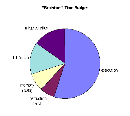
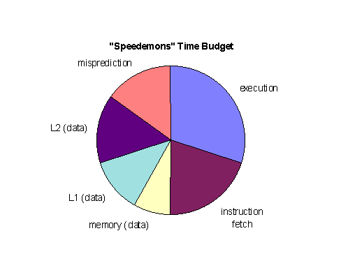
Figure MPSS6: Microprocessor time budget (source: [Sheaffer96])
Legend:
L1/2—First/second level cache.
[Sheaffer96] Sheaffer, G.,
"Trends in Microprocessing,"
Keynote Address,
YU-INFO-96,
Brezovica, Serbia, Yugoslavia,
April 1996.
Veljko Milutinovic
MPS:
IFACT
vm@etf.rs
Ten Example Models of a RISC Design
Models:
UCB RISC
SU MIPS
INTEL i86, i486, i860, i960
MOTOROLA mc68000, mc88100
SGI r4000
SUN sparcV8
DEC alpha21064
IBM power601*
HP pa7*
AMD k5*
References:
[Milicev97] Milicev, D., Petkovic, Z., Raskovic, D., Stefanovic, D., Zivkovic, M., Jelic, D., Robal, M., Jelisavcic, M., Milenkovic, A., Milutinovic, V.,
"Models of Modern Microprocessors,"
IEEE Transactions on Education, 1997.
[Milicev96] http://ubbg.etf.rs/~emiliced/,
University of Belgrade, Belgrade, Serbia, Yugoslavia, 1996.
|

|
Editor: Will Tracz, Loral Federal Systems, MD 0210, Owego, NY 13827; Internet, tracz@lfs.loral.com |
Ten lessons learned from a RISC design
essons can be learned anywhere on earth, and we’ve accumulated a few from our international project—a 64-bit RISC processor design using silicon compilation (with 2.5 million transistors) that took two years to complete. Project teams were located on three continents: a US company provided the hardware description language; a European group (the two of us) was responsible for generating the HDL-based model that correctly described all signals on all pins for each instruction and every operational mode; and a Japanese company generated over 10 Mbytes of tests. Our team’s task was then to successfully pass these tests, after which another US company did the silicon compilation. Finally, another Japanese company did the fabrication. You can imagine the possibilities for complexity! Here are a few of the many lessons we learned.
Lesson #1: It’s tough for just one person to understand everything. A silicon compiler’s essential value is that it enables one person to fully understand a relatively complex design task; however, it’s extremely difficult for one person to manage every detail. In our case, the details were all signals on all pins for every instruction executed in each operational mode. It’s important that future HDL extensions contain language constructs to efficiently express such details!
Lesson #2: Coding rules for silicon compilation are underdeveloped. One nice thing about HDLs is that they let you adequately exploit the full parallelism at the lowest hardware levels for efficient programming. However, current silicon compilers get "confused" with too much parallelism, so the HDL programmer must serialize the description, which negatively affects programmer productivity. The solution? Develop design rules characterized by maximum parallelism yet without negative effects on synthesis efficiency!
Lesson #3: Don’t let silicon compiler warnings get you down. We’ve noticed that many silicon compilers generate correlated warnings. Consequently, a huge number of warnings results in a mere handful of coding rule violations. Therefore, the generated warnings must be orthogonalized!
Lesson #4: Be careful when naming variables. A silicon compiler shouldn’t specify how variable names are created. For example, our register variable names had to start with "r_." This can be confusing, especially of required of the HDL programmers after they’ve mostly completed their task.
Lesson #5: The environment keeps changing. The silicon compiler was fully developed by the time we started our work, but the programming rules that enabled synthesis were not. Consequently, creating rules was a trial-and-error experience. Also, the silicon-compilation design process is still lengthy, so the project requirements are likely to change during the design process. Nothing new!
Lesson #6: Testing is still the bottleneck. The first 90 percent of the project—design—was completed in six months, while the remaining 10 percent—testing—needed another 18 months!
Lesson #7: Beware the NIH problems. People who work in high tech tend to think very highly of themselves, and that characteristic caused some problems of the NIH ("not invented here") variety. When a test failed, entirely too much time was spent trying to determine who made the error rather than getting on with fixing it. The typical reaction was always to blame someone else for the error.
Lesson #8: Working on three continents is both pleasure and pain. If the phone woke you up in the early morning, you knew the call was from Japan. If the phone woke you up late at night, you knew the call was from the USA. After awhile, you learned the best time to send e-mail to get a prompt response. Cultural differences, although a source of fun, can provoke misunderstandings that create hard feelings.
Lesson #9: Time to market is still an issue. A major driver of silicon compiler development is fast time to market. However, the goal has not yet been met to accelerate very sophisticated processor-logic designs adequately. There’s lots of research room for new methodologies in the over-one-million-transistor arena.
Lesson #10: We’re always more clever after the fact! As the saying goes, "hindsight is 20-20." Looking back, it’s obvious that better planning up front would have eliminated many problems (although, unfortunately, none of the above!). Better planning would definitely have reduced the 18 months it took to eliminate the last 10 percent of errors. Also, we’re all now older and wiser, with two years’ more experience!
OUR PROCESSOR DESIGN PROJECT—with all its lessons learned—was one of life’s special experiences. During the two long years of work, one of the project team members passed away, and another one received a beautiful new baby. Sometimes, life resembles engineering so much!
Veljko Milutinovic and Zvezdan Petkovic
University of Belgrade
emilutiv@ubbg.etf.rs